


 Designer’s Notebook: What Designers Need to Know About Manufacturing, Part 2
 The Pulse: Drilling Down on Documentation
 Connect the Dots: Designing for Reality: Prioritizing Manufacturability
iCD Introduces New Materials Planner Software
July 2, 2018 | ICDEstimated reading time: 1 minute
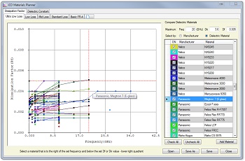
In-Circuit Design Pty Ltd (iCD), Australia, developer of the iCD Design Integrity software, has released the new iCD Materials Planner software to add to the Stackup Planner functionality. This will be rolled out to iCD support customers as an update to their current software.
The Dielectric Materials Library, which complements the iCD Stackup Planner, has
- Over 33,000 rigid and flexible materials up to 100GHz
- Produced by over 60 different manufacturers
- Containing over 700 series of materials
So, it is often a daunting task to ascertain which is the best material for an application. The iCD Materials Planner allows you to compare dielectric materials based on manufacturer, fabricator, frequency, dissipation factor (loss) and dielectric constant. This enables the designer to make an informed decision on which material is best for his application.
Generally the selection metric, for dielectric materials, is the amount of loss that a transmission line can tolerate and this is proportional to the frequency and rise time of the signals. The iCD Materials Planner is subdivided into five default TABs which gives the novice high-speed PCB designer a heads-up as to what to select for his application.
- Ultra Low Loss (Df ≤ 0.005)
- Low Loss (0.005 < Df < 0.010)
- Mid Loss (0.010 < Df < 0.015)
- Standard Loss (0.015 < Df < 0.02)
- Basic FR-4 (Df ≥ 0.02)
This is similar to a typical competitive analysis that a material manufacturer may present for, say, Isola vs Ventec and Rogers, but it is far more comprehensive, with over 60 vendors and 700 series of materials to choose from. Alternatively, a profile for each PCB fabricator that you usually deal with can be set up. This will display the complete range of materials that each Fab shop stocks ranging from basic FR-4 to low loss materials. This also enables the comparison of competitive Fab shop capabilities.
Watch below for a quick demonstration video of the iCD Materials Planner:
About In-Circuit Design Pty Ltd
In-Circuit Design Pty Ltd, based in Australia, developer of the iCD Design Integrity software incorporating the iCD Stackup, PDN and CPW Planner software, is a PCB Design Service Bureau and specialist in board level simulation. For further information or to download a free evaluation of the software, please click here.
Share on:


Suggested Items
Real Time with… IPC APEX EXPO 2024: Ventec Discusses New Pro-bond Family of Advanced Products
05/01/2024 | Real Time with...IPC APEX EXPOChris Hanson, Ventec's Global Head of IMS Technology, outlines the launch of four pro-bond formulas that deliver an outstanding combination of low dissipation factor (Df) with a dielectric constant (Dk) range to maximize the design window for critical PCB parameters. As Chris points out, Pro-bond is designed for low-loss, high-speed applications, while thermal-bond dissipates heat from a component through the board to a heat sink.
IPC's Vision for Empowering PCB Design Engineers
04/30/2024 | Robert Erickson, IPCAs architects of innovation, printed circuit board designers are tasked with translating increasingly complex concepts into tangible designs that power our modern world. IPC provides the necessary community, standards framework, and education to prepare these pioneers as they explore the boundaries of what’s possible, equipping engineers with the knowledge, skills, and resources required to thrive in an increasingly dynamic field.
iNEMI Packaging Tech Topic Series: Role of EDA in Advanced Semiconductor Packaging
04/26/2024 | iNEMIAdvanced semiconductor packaging with heterogenous integration has made on-package integration of multiple chips a crucial part of finding alternatives to transistor scaling. Historically, EDA tools for front-end and back-end design have evolved separately; however, design complexity and the increased number of die-to-die or die-to-substrate interconnections has led to the need for EDA tools that can support integration of overall design planning, implementation, and system analysis in a single cockpit.
Cadence, TSMC Collaborate on Wide-Ranging Innovations to Transform System and Semiconductor Design
04/25/2024 | Cadence Design SystemsCadence Design Systems, Inc. and TSMC have extended their longstanding collaboration by announcing a broad range of innovative technology advancements to accelerate design, including developments ranging from 3D-IC and advanced process nodes to design IP and photonics.
Ansys, TSMC Enable a Multiphysics Platform for Optics and Photonics, Addressing Needs of AI, HPC Silicon Systems
04/25/2024 | PRNewswireAnsys announced a collaboration with TSMC on multiphysics software for TSMC's Compact Universal Photonic Engines (COUPE). COUPE is a cutting-edge Silicon Photonics (SiPh) integration system and Co-Packaged Optics platform that mitigates coupling loss while significantly accelerating chip-to-chip and machine-to-machine communication.