


 Designer’s Notebook: What Designers Need to Know About Manufacturing, Part 2
 The Pulse: Drilling Down on Documentation
 Connect the Dots: Designing for Reality: Prioritizing Manufacturability
Epec Now Offering PCB Layout and Design Services
July 21, 2017 | EpecEstimated reading time: 1 minute
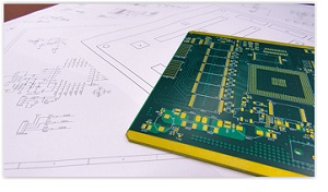
Epec Engineered Technologies, one of America’s oldest printed circuit board (PCB) manufacturers located outside of Boston, Massachusetts, is now offering PCB layout and design services to their customers.
Founded in 1952, Epec has a long history with circuit boards and the PCB industry. Over the past 65 years, Epec has worked on countless circuit board parts for some of the top tier OEMs in the electronics industry. From having PCBs on the Apollo 11 spaceflight, which landed the first humans on the Moon, to their recent advancements in heavy and extreme copper circuit boards, Epec’s sixty-five year history of innovation has truly made them a thought leader amongst the electronics community.
Ed McMahon, CEO of Epec, said, “We have been offering PCB layout and design services a while now, we just never had a large demand for it. In the past when a customer came to us looking for PCB design help, we wouldn’t turn them away; it was just not an advertised offering in our product line.”
Epec’s PCB layout and design services encompass a full design flow including rules driven designs, schematic capture, library development, database construction and verification, signal integrity/design verification, EMI checking and many others.
McMahon added, “We are now seeing more and more companies come to us to help them with their circuit board layout needs. Having the resources in-house allows us to be an extension of our customers engineering teams. We’ve also seen the benefits of customers having their PCB layout and design done by the same company that will be manufacturing their boards as it helps to reduce cost by only designing exactly what they need.”
As Epec continues to expand their PCB supply chain and services, they do so with one goal in mind; to provide their valued customers what they need and when they need it.
About Epec, LLC
Epec Engineered Technologies is the ideal choice for an OEM seeking customized product solutions from a focused and agile partner having supported over 5,000 customers across all sectors of the electronics industry. By providing highly experienced technical resources, a proven manufacturing platform and the fastest delivery in the industry, we are able to provide cost effective and innovative solutions that deliver the highest reliability products to the market faster. Click here for more information.
Share on:


Suggested Items
Designer’s Notebook: What Designers Need to Know About Manufacturing, Part 2
04/24/2024 | Vern Solberg -- Column: Designer's NotebookThe printed circuit board (PCB) is the primary base element for providing the interconnect platform for mounting and electrically joining electronic components. When assessing PCB design complexity, first consider the component area and board area ratio. If the surface area for the component interface is restricted, it may justify adopting multilayer or multilayer sequential buildup (SBU) PCB fabrication to enable a more efficient sub-surface circuit interconnect.
Insulectro’s 'Storekeepers' Extend Their Welcome to Technology Village at IPC APEX EXPO
04/03/2024 | InsulectroInsulectro, the largest distributor of materials for use in the manufacture of PCBs and printed electronics, welcomes attendees to its TECHNOLOGY VILLAGE during this year’s IPC APEX EXPO at the Anaheim Convention Center, April 9-11, 2024.
ENNOVI Introduces a New Flexible Circuit Production Process for Low Voltage Connectivity in EV Battery Cell Contacting Systems
04/03/2024 | PRNewswireENNOVI, a mobility electrification solutions partner, introduces a more advanced and sustainable way of producing flexible circuits for low voltage signals in electric vehicle (EV) battery cell contacting systems.
Heavy Copper PCBs: Bridging the Gap Between Design and Fabrication, Part 1
04/01/2024 | Yash Sutariya, Saturn Electronics ServicesThey call me Sparky. This is due to my talent for getting shocked by a variety of voltages and because I cannot seem to keep my hands out of power control cabinets. While I do not have the time to throw the knife switch to the off position, that doesn’t stop me from sticking screwdrivers into the fuse boxes. In all honesty, I’m lucky to be alive. Fortunately, I also have a talent for building high-voltage heavy copper circuit boards. Since this is where I spend most of my time, I can guide you through some potential design for manufacturability (DFM) hazards you may encounter with heavy copper design.
Trouble in Your Tank: Supporting IC Substrates and Advanced Packaging, Part 5
03/19/2024 | Michael Carano -- Column: Trouble in Your TankDirect metallization systems based on conductive graphite or carbon dispersion are quickly gaining acceptance worldwide. Indeed, the environmental and productivity gains one can achieve with these processes are outstanding. In today’s highly competitive and litigious environment, direct metallization reduces costs associated with compliance, waste treatment, and legal issues related to chemical exposure. What makes these processes leaders in the direct metallization space?